EEET2045 Semiconductor Device Fabrication Sem 1 2022
Hello, dear friend, you can consult us at any time if you have any questions, add WeChat: daixieit
EEET2045 Semiconductor Device Fabrication (PG)
Sem 1 2022
SIMULATION LABORATORY
Provide the fabrication steps and simulation of operation, for the circuit in Figure 1.
ONE ASSESSMENT FOR THESE LABS: SUBMIT A WRITTEN REPORT OR A VIDEO REPORT. STUDENTS ARE ENCOURAGED TO WORK IN PAIRS AND FOR A PAIR BOTH A WRITTEN AND A VIDEO REPORT ARE REQUIRED. DUE AT END OF SEMESTER – WEEK 13 OR A DATE AGREED WITH COURSE COORDINATOR.
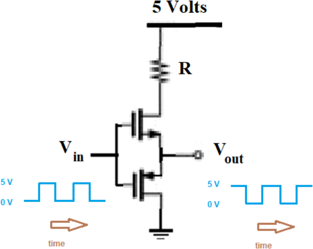
Figure 1: Circuit to be fabricated. NOTE source and substrate are tied (or source and well). Resistor value depends on your student number – see below.

TASK 1:
The fabrication process must satisfy the following requirements
· The circuit is fabricated on the p-type silicon substrate with the doping concentration
NA = 1 x 1016 cm-3.
· Make an n-well by ion implantation and drive-in to make a junction depth of approximately 2.0 mm.
· The p+ layer for the source and the drain of the p-MOSFET has sheet resistance determined by your student number as follows: Sheet Resistance Rsh = First three digits of your student number.
e.g. s3690934 then Rsh = 369 ohms per square
Use Ion Implantation simulation (in given Matlab code ) and the ‘PV Lighthouse’ website to realise the sheet resistance (first three digit of your student number) and find the junction depth. Compare the profile you obtained by ion implantation simulation with the PV lighthouse so they are the same and record the values and the images for your report.
· Do similar to above for the n+ layer of the n-MOSFETs.
· Junction depth should be 0.6 mm for sources and drains (see Microwind)
· Link for PV lighthouse: https://www2.pvlighthouse.com.au/calculators/sheet%20resistance%20calculator/sheet%20resistance%20calculator.aspx
TASK 2:
· Form the resistor by diffusion doping (not ion implantation)
· Use the given Matlab code for simulation of diffusion doping. This should include predeposition first, followed by drive-in.
· For the resistor consider sheet resistance as the last two digits of your student number. If your student number is s3690934 then Rsh = 34 Ω per square
· The resistance is to be considered as the last three digits of your student number. If the student number is s3690934, then R = 934 Ω. If the number of squares for R (using your student number) is less than 10, then double R until the number of squares required is more than 10 (otherwise it will be not appropriate to have corners).
Examples:
1. s3456789 R sh = 89 W, R = 789 W, therefore the number of squares is approximately 9. This is less than 10, therefore R=1578 W, and the number of squares is now approximately 18.
2. s6876943 R sh = 43 W, R = 943 W, therefore the number of squares is approximately 22. So OK as is.
3. s3456989 R sh = 89 W, R = 989 W, therefore the number of squares is approximately 11. So OK.
4. s3456480 R sh = 80 W, R = 480 W, therefore the number of squares is approximately 6. This is less than 10, therefore R=960 W, and the number of squares is now approximately 12.

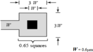
Figure showing how the examples 1 to 4 might be designed, including at least two corners in each.
· Junction depth should be less than 3.0mm
· Use Irvin’s curves (below) for p-diffusion to determine the sheet resistance.
· Adjust the diffusion conditions until you get the desired sheet resistance.
· You need to make at least two corners when designing the resistance
· It is likely that considering correction for corners and diffusion area for contact, that you will not have an integer number for total squares
TASK 3:
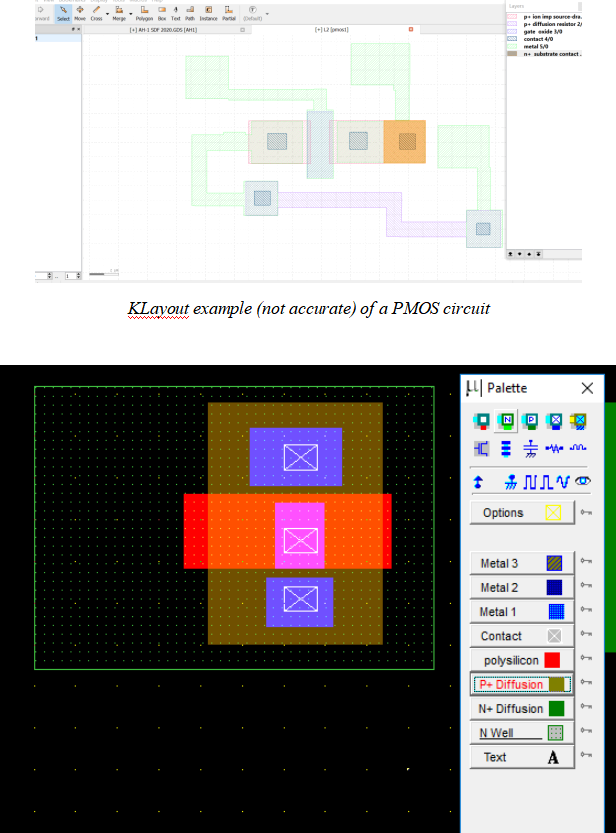
· Use Microwind (and possibly KLayout, but must use Microwind) to produce the mask patterns for the whole circuit.
· Access the licenced version of Microwind in RMIT-Mydesktop
· Assume the technology is 0.6mm (0.6 micron) CMOS. Therefore the smallest line width is W=0.6mm. The PMOS channel length (distance between source and drain is designed for L= 0.6mm but may be less considering lateral diffusion of dopants.
· Make pads that are three times wider than the metal lines and for resistors allow for correction to resistance due to such pads
![]()
· Draw the mask for the oxide etches, the gate oxide and also draw the mask for the metal layer from the design you made.
· Include an n+ substrate contact which is connected to the source (a p+ region) with metal joined across them.
· Show appropriate cross-sections (from Microwind) to demonstrate your design
REFERENCES:
See Lecture notes on CMOS process (lecture file #2), ion implantation and diffusion doping.
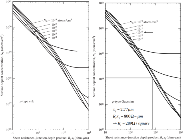
Figure 2: Irvin’s curves for p-type diffusion doping with example shown. You only need the curves on the right. The left side is for predeposition, the right for drive-in.
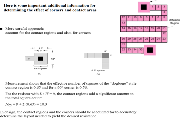
Figure 3: Corner corrections
SUBMISSION
· SUBMIT A WRITTEN REPORT OR A VIDEO REPORT. STUDENTS ARE ENCOURAGED TO WORK IN PAIRS AND FOR A PAIR BOTH A WRITTEN AND A VIDEO REPORT ARE REQUIRED. DUE AT END OF SEMESTER – WEEK 13 OR A DATE AGREED WITH COURSE COORDINATOR
· For report students need to insert the pictures of Matlab simulation and PV lighthouse. Please also need to provide us the approximate values and explain the design of the components (FETs and resistors). Include Microwind layout, cross-sections and simulation of circuit operation.
· For video students need to explain all the above-mentioned points.
· Both report and video have to be submitted at the end of week 13.
· Report can be submitted to Professor Anthony Holland ([email protected])
· Video can be submitted to Professor Anthony Holland ([email protected]).
· The report is named: [name]_[id]_[under-grad].pdf.
2023-06-13