ECE3161 Analogue Electronics Semester One 2022
Hello, dear friend, you can consult us at any time if you have any questions, add WeChat: daixieit
ECE3161
Analogue Electronics
Semester One 2022
Question 1 (40 Marks)
Q1. Part A [20 marks]
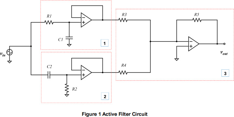
Figure 1 shows an active filter circuit that consists of multiple operational amplifiers, resistors, and capacitors.
1. Identify the function of each sub-circuit in the active filter circuit. [3 marks]
2. Design the circuit in Fig. 1 such that
• the cut-off frequency of sub-circuit 1 is [500 + 10 × last 2 digits of your student ID] Hz.
• the cut off frequency of sub-circuit 2 is [5000 + 100 × last 2 digits of your student ID] Hz.
• the gain of sub-circuit 3 is equal to the first digit of your student ID.
Use standard resistors (±5%) and capacitors (±10%) only. [8 marks]
Example: A student with student ID 12345678 should design the cut-off frequencies of sub-circuits 1 and 2 to be f1 = 500 + 780 = 1280 Hz and f2 = 5000 + 7800 = 12800 Hz. The gain of sub-circuit 3 for this student should be 1.
3. Sketch the frequency response (Bode plot) of each sub-circuit. Clearly show the gain and phase plots and mark the important points. You should plot three separate Bode plots, one for each sub-circuit. [3 marks]
4. Find the expressions for the input and output impedances of the total circuit. [2 marks]
5. A student wants to modify the circuit to improve the steepness of the filters. How could the student achieve this? Draw a new circuit with your proposed modifications to the existing circuit. You do not need to calculate any component values. [4 marks]
Q1. Part B [20 marks]
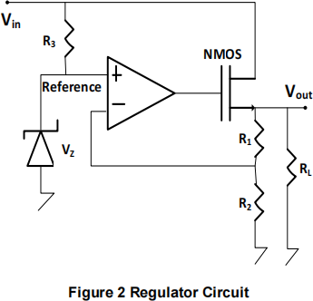
Figure 2 shows a regulator circuit that has an input DC voltage of 12 V (Vin=12 V). The regulator circuit should be designed to provide an output voltage of 9 V, Vout = 9V to a 50-ohm load (RL= 50![]() ).
).
1. Identify suitable values of R1 , R2 , R3 and Vz so the regulator circuit can function as desired. [6 marks]
2. Following part 1, calculate the input current, the drain current of the NMOS, and the output current. Label these currents on the circuit diagram. [9 marks]
3. What is the power dissipated in this regulator circuit, excluding the load? [5 marks]
Question 2 (60 marks)
Use the schematic circuit diagram of the internal workings of the LH0061 op-amp provided on Moodle.
The LH0061 is topologically similar to many op-amps but with a “power” output stage added suitable for inductive loads. The base currents to drive the output transistors (Q13, Q15) are the power supplies to the first part of the circuit.
Instructions for analysis:
1. We are not interested in the external feedback circuits around the op-amp; but the simulation will require a load and input signals.
2. If the exact operation of the circuit is not clear, make reasonable assumptions and explain them.
3. Ignore the input Emitter Followers (Q1, Q4) and R3, R4: Assume the bases of Q2 and Q3 are the inputs. D1 and D2 can be ignored.
4. Note that a Zener diode (D3) is used to provide a constant voltage reference as marked.
5. Assume all current mirrors have 1:1 ratios. Assume all BJTs are identical in characteristics (apart from PNPs having complementary characteristics to NPNs)
6. Assume R11 and R12 are 1000 Ω .
7. You can ignore the short-circuit protection circuitry: that is, remove Q12 and Q14, and set the Rsc resistors to zero (between SC+ and V+, and between SC- and V-).
8. To operate properly, this op-amp has a 0-volt connection (GND) to R14.
9. Initially ignore C1. Assume Cc is zero (COMP to OUTPUT pins).
Part A: Analysis (30 marks)
i. Identify and name the main sub-circuits of the schematic, such as: current mirrors (types), differential pairs, gain circuits, output stages. Circle the sub-circuits, or draw a simplified diagram representing sub-circuits as blocks, where possible. [8 marks]
ii. Provide an explanation of the purpose of each component in any two sub-circuits, such as: “Rx converts a collector current to a voltage for the next stage of the circuit”, or “Qx is a common collector amplifier with emitter degeneration that amplifies xxxx to drive the input of the next stage xxxx” . You may have to label the circuit schematic. [8 marks]
iii. Analyse the DC bias (quiescent) conditions for the circuit from the inputs, to the bases of Q10 and Q11. Find the collector voltages of Q2, Q3, and Q5 through Q9. Use appropriate simplifications and approximations for the transistor models. You can also assume typical input and output voltages for an op-amp, and ±15 V dual rail power supplies (V+, V-). [8 marks]
iv. Consider the input differential pair. Estimate its AC small-signal transconductance at the above bias conditions. Calculate its differential voltage gain. Show and explain your working. [6 marks]
You will be awarded marks for using appropriate models, approximations and simplifications of the active components, and explaining why they are appropriate.
Part B: Simulation (30 Marks)
Use LTspice to simulate the internal circuit of the op-amp.
Instructions for simulation:
• We are not interested in the external feedback circuits around the op-amp; but the simulation will require a load and input signals.
• Use the generic NPN and PNP transistors in the LTspice component library. Be careful of the orientation of the PNP transistors; they may have to be rotated.
• Ignore the input Emitter Followers (Q1, Q4) and R3, R4: Assume the bases of Q2 and Q3 are the inputs. D1 and D2 can be ignored.
• Assume the output stage biasing diodes are diode-connected NPN transistors.
• Assume R11 and R12 are 1000 Ω .
• Use a 50-ohm load to ground (GND, 0 V) at the output of the op-amp (OUTPUT).
• Remove Q12 and Q14 (current limiting circuits), and set the Rsc resistors to zero (between SC+ and V+, and between SC- and V-).
• To operate properly, this op-amp has a 0-volt connection (GND) to R14.
• Initially ignore C1. Assume Cc is zero (COMP to OUTPUT pins).
• Initially apply a 5-mV p-p 1-kHz sinewave of the op-amp, and ground the non-inverting (NON- INV) input.
• Simulate with a maximum timestep of 1u (1μs) when in transient simulation mode.
• Do not expect your simulations to predict the same performance as that given in the data- sheet.
i. First, simulate the operating point (.op) of the circuit (a.k.a. bias point, quiescent point, Q- point).
a. Capture the schematic for your report. Also, submit your *.asc schematic file via Moodle. [4 marks]
b. Slightly adjust R1 so the OUTPUT voltage is within 600 mV of GND. State R1’s value. [4 marks]
c. Identify two interesting voltages, and mark on your schematic. How closely do these
voltages agree with your calculations in Part A (iii)?
Explain any significant discrepancies. [4 marks]
Hint: Do not simply screen grab a result (like a long list of voltages) and expect the examiners
to find the interesting result for you in the list (highlight them): clearly label which nodes you are monitoring on your schematic circuit for easy cross-referencing. You can use the Place .op Data Label (right click on a wire) command.
ii. Secondly, simulate the internal circuit’s transient (.tran) response to a small-value 1-kHz sinusoidal input to the Inverting input (INV). Ground the other input. The mean output voltage may be slightly different to the one found in the operating point simulation. Select the amplitude of the input for maximum output just before clipping.
![]()
Capture and explain at least three waveforms of important and interesting node voltages and/or branch currents. Calculate the open-loop voltage gain of the op-amp. [6 marks]
iii. Now set C1 to be 20 pF. Use “AC Analysis” (.ac) to produce a gain and phase plot for the amplifier (output/input) up to a frequency at least 2 decades beyond the dominant pole.
a. Capture the gain and phase plots. [2 marks]
![]() b. What is the frequency of the dominant pole? [2 marks]
b. What is the frequency of the dominant pole? [2 marks]
c. Is the op-amp stable when configured as a unity-gain buffer? Show reasoning or evidence to justify your answer. [2 marks]
iv. Using a simulation with the load removed, determine the output impedance of the op-amp at
1 kHz when no external feedback is used. Include your schematic. [4 marks]
v. Which internal component(s) mainly determine the output impedance for this op-amp? [2 marks]
2023-06-06