ELEC4614 POWER ELECTRONICS FINAL EXAMINATION Term 1, 2022
Hello, dear friend, you can consult us at any time if you have any questions, add WeChat: daixieit
FINAL EXAMINATION
Term 1, 2022
ELEC4614
POWER ELECTRONICS
QUESTION 1 [20 Marks]
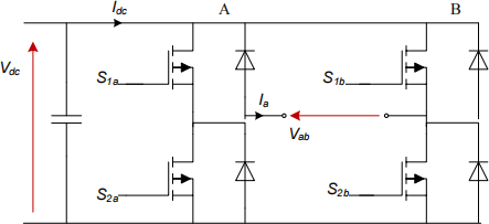
Figure 1
a) Using the H-bridge circuit, shown in Figure 1, in the inverting mode, it is possible to generate three different instantaneous voltage values for, Vab, (the load voltage). Assuming that the current is flowing in the load in the direction shown, Ia, list which switch pairs need to be turned on in order to generate each of the three possible voltage values. [3 marks]
b) What type of converter is the H-bridge from the point of view of the transformation ratio Vdc/Vab (buck, boost or buck-boost) assuming a current source is connected between the mid-points of the two phase legs and supplies a constant current Ia in the direction shown in Figure 1? [3 marks]

Figure 2 showing pulse-width modulation scheme
c) Figure 2 shows the PWM scheme for the H bridge inverter shown in Figure 1. For each set of parameter values listed in i. to iii., sketch the output current waveforms, Ia, and the input current, Idc, that results over a switching period and indicate which direction the power is flowing in the dc supply for each state of the inverter. Assume the switching period is 100µs, the PWM carrier is a triangular waveform as shown in Figure 2, the dc voltage is 200V, and the RL load is R=2Ω and L= 500 µH. Also assume that the load current has reached a steady-state. In your sketch ensure that you mark the important times and current values at these times.
i. Bridge leg A uses a modulation index of 0.75, and bridge leg B uses a modulation index of 0.25. [6 marks]
ii. Bridge leg A uses a modulation index of 0.5, and bridge leg B uses a modulation index of 0. [2 marks]
iii. Bridge leg A uses a modulation index of 0.85, and bridge leg B uses a modulation index of 0.35. [2 marks]
d) From the sketched waveform answers in part c), describe which pair of modulation indices for bridge leg A and B results in the lowest overall ripple in the load current Ia, and which might produce the lowest losses in the switching device. [4 marks]
QUESTION 2 [20 Marks]
A non-isolated dc-dc converter is required to supply a load at 48V with an output current that ranges from 0. 1A to 1A. The switching frequency is to be 100kHz and the input voltage a steady dc of 12V. You are asked to compare the performance and operation of the boost converter and buck-boost converter. For each converter the inductor has an inductance of 150 μH and the output capacitor a capacitance 100 μF.
a) Draw the circuit diagrams of the boost and the buck-boost converter circuits using the component values given above. [4 marks]
b) Show that each converter will operate in CCM for the given range of output currents expected. [4 marks]
c) Plot the inductor current waveforms at full load (1A) for each converter and compare their peak inductor currents. [4 marks]
d) Plot the inductor current waveforms at minimum load (0. 1A) for each converter and compare their peak inductor currents. Comment on the margin between DCM and CCM for each converter. [4 marks]
e) Plot the capacitor current waveforms at full load (1A) for each converter and compare their peak values. [4 marks]
QUESTION 3 [20 Marks]
a) Draw the circuit diagram of the flyback converter circuit including the dots on the windings and the magnetising inductance. [3 marks]
b) Derive the following expression that relates the input and output voltages (Vd and Vo respectively) of the flyback converter to the modulation index D for DCM:
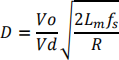
where the parameters take on their usual definitions. [6 marks]
c) A flyback converter is required to generate a 48V DC output from a 600V DC input voltage. The coupled coil in the flyback converter has a turns ratio of 10:1 (N1 :N2). The coupled coil has a primary inductance of 2mH. The rated output current is 0.5A. The switching frequency is 100 kHz.
i. Calculate the required D to generate 48V assuming an output current of 0.5A. [3 marks]
ii. Draw the waveforms of the resultant input current, diode current and output capacitor current clearly showing the time on the x-axis and the current values on the y-axis. [5 marks]
iii. Determine the load resistance required to achieve an output voltage of 48V with D set to 0.2. [3 marks]
QUESTION 4 [20 Marks]
The MOSFET switch shown in figure 3 is switched at a frequency of 100 kHz and has an Rds(on)=20mΩ. In the circuit shown, the input voltage is 200V and the intended load voltage is 150V. The load current will be 30A if the average load voltage is 150V. The FET voltage rise time is 15ns and fall time is 20ns at turn-off and turn-off respectively. The current rise time and fall time are both 25ns.

a) Figure 3 is a single-end dc-dc converter that is controlling the average voltage, VL, across the load inductor. On graph paper, sketch voltage and current waveforms for the MOSFET, the load and the diode during the turn-on and the turn-off transient. You may assume that the turn-on and turn-off transients of voltage and current of the FET occur along straight lines and that the load current remains constant during the switching transient. [5 marks]
b) Two diodes are to be assessed. Diode, DF, is a Schottky diode with an on-state voltage of 0.4V and a leakage current of 50mA. An alternative pn fast recovery diode is available that has a forward voltage drop of 1. 1V with a recovery time, trr = 50ns and Qrr = 50nC. Calculate the power loss in each diode including only the conduction loss and any reverse leakage current. [4 marks]
c) Calculate the total loss in the FET assuming a modulation index of 0.75 and accounting for conduction and switching loss. [5 marks]
d) Calculate and compare the efficiency of the circuit with the Schottky and the pn fast recovery diode. [3 marks]
e) Assuming an ambient temperature of 50oC, what is the maximum thermal resistance from junction to ambient for the Schottky and pn fast recovery diode to maintain the junction temperature at 70oC? [3 marks]
2023-05-07