Exam Announcement - ELEC4614
Hello, dear friend, you can consult us at any time if you have any questions, add WeChat: daixieit
Exam Announcement - ELEC4614
Please read the following instructions carefully and have them accessible during the exam for reference.
• Your final exams for ELEC4614 is on Wednesday 5th May 2021.
• The exam will take place 1:50-4:30 pm on the day and you will have 160 minutes in total to complete the exam including reading time (10 mins), exam time (120 mins) and upload time (30 mins).
• The exam will be a timed online exam via Moodle and will be treated as an open book exam.
• Note that by submitting the exam you verify that it represents your own work and that you
did not give or receive assistance in any way that would violate the UNSW Student Code (https://student.unsw.edu.au/conduct).
• The exam is similar to previous final exam formats for ELEC4614 with four questions from which you choose three.
• For each question, you will upload every page of your solution as an image in the respective blocks.
• Please take a photo using for example your phone camera and upload the images.
• If convenient, you can use your tablet devices to work out the answers and upload them as pdf.
• Scanning your documents will take more time and is not recommended. This will not be taken as an excuse for late submission.
• Upload your answer sheets as and when you complete each question during the exam – Do not wait until the end.
• In case you did not arrive at the full solution and wish to attempt the next question, you are recommended to upload all your workings, before going to the next question. You can always come back and upload the correct solution again.
• Late submissions are not possible. Moodle will close automatically.
• In case you fail to upload, say the last question due to reasons of Moodle issues, you may send the last question via email within 5 min of finishing the exam.
• Late submissions will however incur penalties.
• If in case, you have failed to upload all answers in Moodle, and you submit all answers via email, these will not be marked, and your grade becomes “FL” .
• A Teams session will be setup for the duration of the exam to answer any clarifying questions during the exam.
• You may apply for special consideration (SC) if you fail to submit the final exam due to technical issues. Please refer to the guidelines providedhereand go through “Steps to follow for online assessments” .
• If you have technical difficulties during the exam, you need to let me know immediately via the Teams session.
• To apply for SC, take as many screenshots as possible of the issue including error messages, timestamped speed tests , power outage maps, etc. and add them as supporting documents.
• SC application should be made immediately after the final exam close, i.e. 4:40 pm on 5th May.
![]() QUESTION 1 [20 Marks]
QUESTION 1 [20 Marks]

Figure 1
a) Using the H-bridge circuit shown in Figure 1 it is possible to generate three different voltage values, Vab, across the load. Assuming the current is flowing in the load in the direction shown, Ia, list which switch pairs need to be turned on in order to generate each of the three possible voltage values. [5 marks]
b) State what type of converter is the H-bridge from the point of view of the transformation ratio between Vab and Vdc (buck, boost or buck-boost) assuming a current source is connected between the mid-points of the two phase legs and supplies a constant current Ia in the direction shown in Figure 1? Explain your answer. [4 marks]
c) If bridge leg A is switched using PWM with a modulation index of 0.75, and bridge leg B switched with a modulation index of 0.25, and the current Ia is -2A, sketch the input current Idc that results over a switching period and indicate which direction power is flowing. Assume the switching period is 100µs and the inductance of the load is sufficient to assume that the current Ia is constant. [4 marks]
d) If an emergency stop procedure results in all four switches being turned-off, describe what happens to the energy in the load including a description of the path load current would form in the inverter once all the switches are off. Assume the load is inductive (10mH) and is carrying 10A of current, and the dc link is 200V with a total dc link capacitance of 1mF, at the instant the procedure disables the switches. [4 marks]
e) In the circumstances of part d) calculate the rise in the dc link voltage that would occur. [3 marks]
QUESTION 2 [20 Marks]
A non-isolated dc-dc converter is required to supply a load at 48V with an output current that ranges from 0. 1A to 1A. The switching frequency is to be 100kHz and the input voltage a steady dc of 12V. You are asked to compare the performance and operation of the boost converter and buck-boost converter. For each converter the inductor has an inductance of 150 μH and the output capacitor a capacitance 100 μF.
a) Draw the circuit diagrams of the boost and the buck-boost converter circuits using the component values given above. [4 marks]
b) Show that each converter will operate in CCM for the given range of output currents expected. [4 marks]
c) Plot the inductor current waveforms at full load (1A) for each converter and compare their peak inductor currents. [2 marks]
d) Plot the inductor current waveforms at minimum load (0. 1A) for each converter and
compare their peak inductor currents. Comment on the margin between DCM and CCM for each converter. [4 marks]
e) Plot the capacitor current waveforms at full load (1A) for each converter and compare their peak values. [4 marks]
f) On the basis of the analysis in parts c)-e), state which converter offers the better solution and why. [2 marks]
QUESTION 3 [20 Marks]
a) Draw the circuit diagram of the flyback converter circuit including the dots on the windings and the magnetising inductance. [3 marks]
b) Derive the following expression that relates the input and output voltages ( Vd and Vo respectively) of the flyback converter to the modulation index D for DCM:
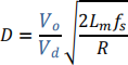
where the parameters take on their usual definitions. [6 marks]
c) A flyback converter is required to generate a 24V DC output from a 400V DC input voltage. The coupled coil in the flyback converter has a turns ratio of 16:1 (N1 :N2). The coupled coil has a primary inductance of 2mH. The rated output current is 1A. The switching frequency is 100 kHz.
i. Calculate the required D to generate 24V assuming an output current of 1A. [3 marks]
ii. Draw the waveforms of the resultant input current, diode current and capacitor current clearly showing the time on the x-axis and the current values on the y- axis. [5 marks]
iii. Determine the load resistance required to achieve an output voltage of 24V with D set to 0.4. [3 marks]
QUESTION 4 [20 Marks]
The MOSFET switch in Figure 4 is a gallium-nitride (GaN) FET device. It can be switched at a frequency of 1 MHz and has an Rds(on)=10mΩ . In the circuit shown, the input voltage is 60V and the intended load voltage is 15V. The load current will be 30A if the average load voltage is 15V. The FET voltage fall time is 5ns and rise time is 10ns at turn-on and turn-off respectively. The current rise time and fall time are both 15ns.
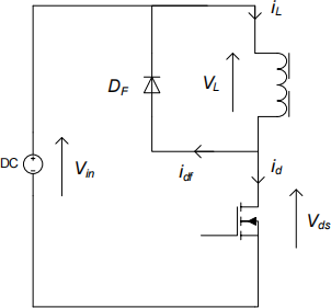
a) Figure 4 is a single-end dc-dc converter that is controlling the average voltage, VL, across the load inductor. On graph paper, sketch voltage and current waveforms for the MOSFET, the load and the diode during the turn-on and the turn-off transient. You may assume that the turn-on and turn-off transients of voltage and current of the FET occur along straight lines and that the load current remains constant during the switching transient. [5 marks]
b) Two diodes are to be assessed. Diode, DF, is a Schottky diode with an on-state voltage of 0.5V and a leakage current of 50mA. An alternative pn fast recovery diode is available that has a forward voltage drop of 1. 1V with a recovery time, trr = 50ns and Qrr = 50nC. Calculate the power loss in each diode which may include conduction loss, reverse leakage current. [4 marks]
c) Calculate the total loss in the FET assuming a modulation index of 0.25. [5 marks]
d) Calculate and compare the efficiency of the circuit with the Schottky and the pn fast recovery diode. [3 marks]
e) Assuming an ambient temperature of 50oC, what is the maximum junction-to-ambient thermal resistance for the Schottky diode and the pn fast recovery diode to maintain the junction temperature at 70oC? [3 marks]
2023-05-07