CNIT 17600 - Intro Computer Architecture - Boolean Algebra Lab
Hello, dear friend, you can consult us at any time if you have any questions, add WeChat: daixieit
CNIT 17600 - Intro Computer Architecture - Boolean Algebra Lab
Boolean Algebra Lab - Part II
Activity Overview
In today’s lab we will the Logic Blocks to build combinatorial and sequential circuits that represent the types of circuits used to build complex computing systems and components of systems.
Combinatorial Circuits
The first circuit we will build using only AND, OR, and NOT gates represents the following
Boolean equation:
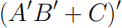
The circuit diagram for this is below:
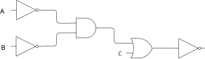
Figure 1: Combinatorial Circuit 1
Create the truth table for this circuit and include it in your lab report. Include a labeled snip of your completed circuit. Summarize the truth table - under what conditions does this gate result in true?
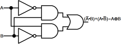
Next, create the following circuit using only three gate blocks from the set of AND, OR or NOT. Determine the truth table for this circuit and include it in your lab report. Compare the results of this circuit to the first combinatorial circuit, under what conditions does this circuit result in true? Using the Boolean laws we have discussed in class, explain the similarities and differences in the two circuits.
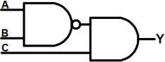
Figure 2: Combinatorial Circuit 2
Sequential Circuits
Ring Oscillator
Next we will build a oscillator. These are circuits that are used to build clocks. The output periodically and repetitively fluctuates. This is accomplished by stringing together an odd number of NOT gates plus some feedback. You will need the following pieces:
• Three (3) NOT gates
• One (1) OR gate
• One (1) switch
The feedback will come when the output of the final NOT gate in the chain is directed back as input into the first NOT gate in the chain. In order to accomplish this using logic.ly, you will need to take the input of a switch, and use it as one of the inputs into an OR gate. The output from the final NOT gate will become the second input into the OR gate. The OR gate will then send its output to the first NOT gate. Build this cir- cuit. Note that logic.ly will show an error in the circuit until you turn it on for the first time.
This circuit will not have a truth table, since its only input is 1. However, it will have a state table where the previous output will lead to the current output. Include this state table in your lab submission. Then, answer the following: How fast is the output of the last NOT gate blinking? Determine the rate as accurately as you can. Include a labeled snip of your first ring oscillator in your report.
Increase the number of NOT gates in the circuit. Determine the rate of blinking with an increase in the number of not gates. It is important to think about these problems scientifically. To collect this data, consider if there is any technology you can use to do so accurately when the blinking rate is perhaps too fast for the human eye. Also consider that multiple trials and calculating an average is an important scientific tool for accurate data collection. Explain how you collected your data in your lab report. How many gates did you use and what was the blinking rate? Draw a conclusion about the relationship here in clock speed and numbers of gates. Include a labeled snip your longer ring oscillator in your report.
SR Flip Flop
The next sequential circuit we will build is a basic form of memory. We will create an SR Flip Flop/Latch. Even though logic.ly exposes a single component block diagram for a SR Flip-Flop, we will build it using only NOR gates. The layout of the circuit for this is given below. When you build this, you will have two inputs, one of which will be your Set, the other will be your Reset. When you build it, determine which input you will refer to as S and which to R. It doesn’t matter which is which, as long as you are consistent.
Create and fill in the values for a state table which includes values for S, R, the Previous Q, the Current Q, and Current Q’.
Figure 3: SR Flip Flop
Include a labeled snip of your completed S/R Flip Flop in your lab submission.
SR Flip Flop with DeMorgan’s Law
Using DeMorgan’s Law, use AND gates (and any other required components) to build the SR Flip Flop. Include a labeled snip of your completed circuit in your lab submission.
The XNOR Gate
Since this is such an important gate for data integrity (error checking) and cryptography, it’s worth attempting to build one. We are going to limit ourselves to ANDs, ORs, and NOTs, this is a semi-complex gate to build. The circuit diagram is below.
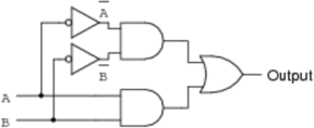
Figure 4: XNOR Circuit with ANDs, ORs, NOTs Only
Build this circuit on logic.ly and include a labeled snip in your report.
Additional Circuit Practice
Examine the circuit diagram below.
Build this gate with logic.ly, take a snip for your report. Create a truth table that demon- strates the outputs associated with each combination of inputs. In your own words, describe when the resulting output of this circuit is true.
Compare the design and output of this circuit to the design and output of the XOR Gate.
The Report
Please be sure to label all your snips so that it is clear what each represents. Truth Tables should also be labeled so that it is clear which circuit they are associated with. We will not assume you have matched these correctly.
2023-02-24