EL 4930 - System-on-Chip Design Spring 2023 Homework 2
Hello, dear friend, you can consult us at any time if you have any questions, add WeChat: daixieit
EL 4930 - System-on-Chip Design
Spring 2023
Homework 2
The Lab is a group assignment
Total: 100 points
(Deadline: 02.19.2023, 11.59pm)
Objective:
The goal of this lab is to have hands-on experience in System-on-Chip design, including peripheral IP integration, bus protocol, and system-level debugging. Here, you will use Xilinx Microblaze soft core processor and build SoC in the Artix-7 FPGA. Then, you have to write the C applications that will run on the Microblaze processor.
Tools and Hardwares required:
1. Xilinx Vivado tool is required for this lab.
2. The BASYS 3 board will be used which has an ARTIX 7 FPGA.
3. A USB- UART cable to program the board and display the output in the terminal
Task Description:
This homework has four parts. Each part is described below with its corresponding points distribution.
Task 1: Getting Started with Microblaze 20 Points
In this task, you must implement a simple SoC using a Microblaze processor, its memory, and UART. The high-level block diagram of the SoC is given below.

Figure 1: A simple SoC
Use the following link step by step and run the Hello World C application. Use the UART terminal to print your C application output. Here, the local memory is used to save the instruction and data of the C program. The UART is used to send the output to the terminal of your computer.
https://digilent.com/reference/learn/programmable-logic/tutorials/basys-3-getting-started-with- microblaze/start
Make a video of running hello world in the terminal.
Task 2: AXI peripheral IP integration 20 Points
In this task, you will integrate an IP in the AXI bus of your SoC developed in Task 2. We have provided a VHDL implementation of 128-bit RSA and its testbench. The module implements the following computation.
C = de mod m
Here, d is input data (indata), e is exponent value (inExp), m is modulo value (inMod), and C is cypher value (cypher). The VHDL top module also has ds, clk, reset and ready signal. Here, ds signal acts as a go signal. Try to run the simulation using the testbench and see if you can see the expected cypher value. The expected cypher value is given as a comment in the testbench.
Now, Create a AXI peripheral IP of the RSA and package it in Vivado. To learn how to package AXI peripheral IP, you can follow the given provided link below.
https://www.fpgadeveloper.com/2014/08/creating-a-custom-ip-block-in-vivado.html/
Then, after packaging the RSA IP, connect it to the AXI bus. Now, you will require two slaves of the AXI bus. You can configure the number of Master and slave ports of AXI Bus in Vivado. The high-level block diagram will look like the following.

Figure 2: SoC with RSA connected to AXI bus
Next, you have to write a C program that will send input data to RSA module and get back the cypher value and print it in the terminal. You must use the exact same input data used in the testbench and get
the cypher value generated by the testbench simulation to verify that the IP integration works correctly.
Make a video demonstrating the running C program on UART terminal.
Task 3: APB peripheral IP integration 25 Points
This time you must use the same RSA module and package it as an APB peripheral IP which means the IP will have an APB interface instead of AXI. We have provided the APB specification document to understand the APB protocol. Please read the I/O signals of APB and properly write the APB wrapper RTL code which will instantiate the RSA top module. Then package it in Vivado as an IP.
Next, you have to add the IP in the AXI bus. As the Microblaze does not have an APB interface, we have to use AXI-APB bridge found in the Vivado IP catalogue. The AXI-APB bridge transforms the AXI signals to APB signals. The high-level block diagram is the following .
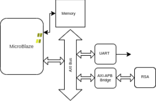
Figure 3: SoC with RSA as an APB peripheral
Please try to reuse the C program written for task 3 and see if you get the correct cypher value. Be sure to use the correct base address found in the address editor of your SoC design in the Vivado.
Again, make a video demonstration showing the Vivado design and the terminal output.
Task 4: APB Bus implementation 25 Points
In this task, you will implement the APB bus according to the provided APB Bus protocol specification. This bus will have one master and three slave interfaces. The master interface will be connected to the AXI- APB bridge. Three IPs will be connected to the three slave interfaces. Three IPs are RSA, Booth multiplier, and Median Filter. You will reuse the packaged RSA module from task 4. The RTL code of booth multiplier and Median filter IPs are provided with corresponding testbenches. Please develop the APB wrapper for these IPs and package those by following the steps used in task 4. The high-level block design will look like the following.

Figure 4: SoC with APB bus and three slave IPs
You have to write a C application that will send input data to the three IPs one by one and get the output . The input values must be used taken from the testbench and output should match found in the testbench simulation. You don’t have to understand the internal logic and implementation of the IPs. The purpose
of this task is to check that the APB bus implementation is correct .
Make a video demonstrating the Vivado design and terminal output.
Note: If you need to debug your system, you can use the system level ILA for tracking the data transfer between the components. You can change the ILA interface, either AXI or APB whatever you need.
https://docs.xilinx.com/v/u/en-US/pg261-system-ila
Submission Guidelines:
1. Include all project files organized in folders.
2. All video demonstrations of the tasks mentioned above.
3. A short report describing what problems you faced, what you have learnt, and work distribution among teammates.
Grading Rubrics:
Implementation tasks ---- 90%
Report ---- 10%
2023-02-24