CNIT 17600 - Intro Computer Architecture - Boolean Algebra Lab
Hello, dear friend, you can consult us at any time if you have any questions, add WeChat: daixieit
CNIT 17600 - Intro Computer Architecture
Boolean Algebra Lab - Part I
1 Activity Overview
For this lab we will be using a website called logic.ly. This site is designed to allow anyone to use logic gates to build circuits. Though there is a for pay option, we will not be using it for our lab. We will take advantage of their free offerings.
The logic.ly site has several control panels on the left side of the screen that are of in- terest and use to us. The first is the input panel. There, we will find toggle switches, which will be our basic input/output. You can experiment with circuits to determine which position allows the switch to be considered on. Then there is the output control panel. We will be using the light bulb for our output, however you are free to play and ex- periment with the other option. Finally, there is also a logic gates panel, which contains all the basic gates we will use (and some we will not use). See the snips of these panels below. Drag and drop the desired component onto the drawing grid, use your mouse to click on a connection dot and draw a line to the point of the next component you wish to connect to.

Figure 1: Input Control Panel from logic.ly
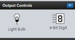
Figure 2: Output Control Panel from logic.ly
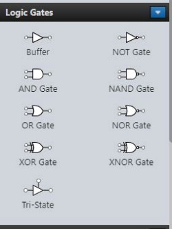
Figure 3: Logic Gates Panel from logic.ly
To read the output of a circuit, the light will glow if the output of the whole circuit is true, and will be unlit if it is false. The intermediate steps will be blue if they are true. See the figures below.

Figure 4: Example AND Gate with all Connections False from logic.ly

Figure 5: Example AND Gate with One True Input Line from logic.ly
Important Note: We differentiate between logic gates and the peripheral building com- ponents (input and output components). When tasked with building a circuit using, for example, no more than two logic gate components, you can use two toggle switches, a light output, etc., but only two logic gates (AND, OR, or NOT).
2 Three Input AND
A three input AND gate is much like a two input version, except it determines whether three input values are all true or not. As a single entity it can be illustrated as a single AND gate with three input lines and a single output line (see below). It can also be illustrated as a circuit of two individual AND gates. Using only two input logic gates, attempt to build the three input AND gate and draw its truth table.
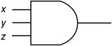
Figure 6: Three Input AND Symbol
With your lab report, submit the labeled truth table and a labeled snip of your completed logic block circuit. Each figure in this document demonstrates how to label images ap- propriately. If you do not label your images properly, there will be no assumptions made about what you “intend” to communicate with the image. Without an image label, many questions will receive zero points of credit. This is important now, and in future labs.
3 NAND & NOR
In our lecture notes, we see that there is a way to construct all the logic gates using only NAND and NOR gates. However, imagine that our logic block panel only contains AND, OR, and NOT gates. Can we do the opposite (of constructing everything from NAND and NOR gates) and construct NAND and NOR gates using the others?
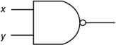
Figure 7: NAND Symbol
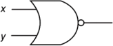
Figure 8: NOR Symbol
First, using two gate components only, create a circuit that is logically equivalent to a NAND gate. Take a snip of this circuit. Repeat this process to create a NOR gate.
Then, using three or more gate components, create a circuit that is logically equivalent to a NAND gate. Take a snip of your circuit. Repeat this process to create a NOR gate equivalent.
How do the results you found relate to DeMorgan’s Law? Answer clearly in your report.
4 Non-Inverting Buffer
A NOT gate is also known as an inverting buffer. A non-inverting buffer, then, does not find the opposite of its input, it simply takes an input value and outputs the same value.
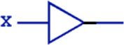
Figure 9: Non-Inverting Buffer Symbol
With the restriction of only using AND, OR, or NOT gates, build a non-inverting buffer. Take a photo and include in your report.
Which of the Boolean laws can be used to explain why your circuit works as a non-inverting buffer. Explain your answer.
5 Report & Administrative Stuff
Turn in your lab report with all images and answers carefully labeled and described.
2023-02-15